Meet SIRIUS: our fully-automatic Photonic Test Probing (PTP) system. Today, testing is done with low levels of automation. PhD’s and R&D Engineers typically perform these tests in a lab environment. This makes the testing process costly and hard to scale for larger batches. SIRIUS performs optical and electrical testing at the front-end production process of Photonic Integrated Circuits (PICs).
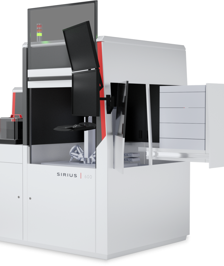

Packaging is the most expensive process step of manufacturing PICs. Knowing which circuits are good enough for packaging saves a lot of costs. With SIRIUS, these circuits are tested and identified so only the right PICs are packaged. The scale-up of the photonics market is supported by automatic optical and electrical probing. The demand for PICs is increasing by the year. A high level of automation in testing offers the competitive edge integrated photonics companies are looking for.
Manual probing is time consuming and slow to set up. This is a major bottleneck for the scale-up of integrated photonics production. A scalable probing solution is required to prevent this bottleneck and to improve yield.
SIRIUS provides you with simultaneous optical and electrical wafer-level tests. The amount of available test data is therefore drastically improved. This helps PIC designers to improve their designs and the foundries to improve their Process Development Kits (PDK). Process engineers will also have new and enhanced insights to improve their process.


Optical probes are used to perform surface and trench coupling. Different methods are employed to couple light in-and-out of the PIC. For surface coupling, PIC grating couplers are employed. For trench coupling SIRIUS supports total internal reflection of optical probes, lensed fibers and 3D printed optical periscopes.
Any questions about automatic test probing of PICs? Use the contact form and we will answer them within 1 working day.
Get in touch
SIRIUS is built for the challenges of today and tomorrow. The architecture of the Photonic Test Prober foresees the scalability that will be necessary in the coming future. This results in lower costs for scaling when needed. Features such as a modular build, higher quantity of measurement channels and faster exchange of production data makes our system unique.
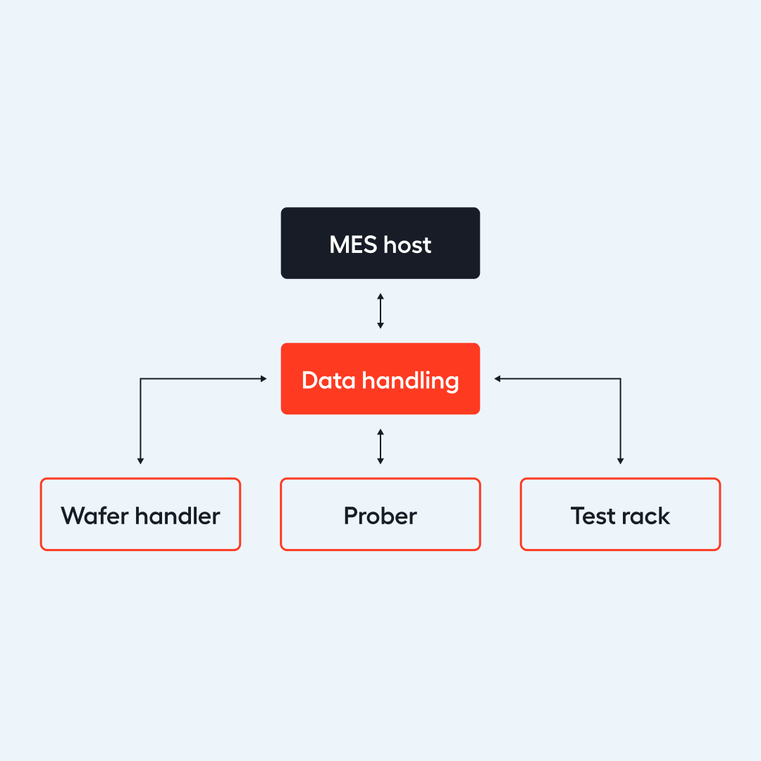
Data is incredibly valuable in today’s manufacturing world. Everything that is done, is driven by data. It is used to set, assess and improve processes. Data exchange is done via the SECS GEM protocol and transfers:
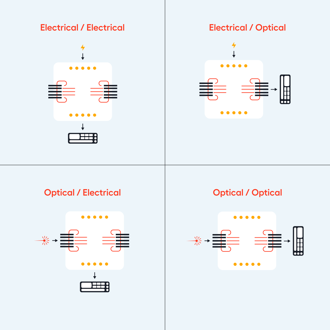
Simultaneous optical and electrical probing and a combination of these methods are supported. Electrical probe cards and optical probes are easily exchangeable within 30 minutes. The probing strategies that can be used are electrical – electrical, electrical – optical, optical – electrical and optical – optical.
 DOWNLOAD
Ramp up your Photonic Integrated Circuit production with fast changeover times and identify KGDs. Various I/O configurations can be used for testing.

