Helios is a Photonic Visual Inspection Tool designed for wafer level inspection. The tool automates optical inspection and analysis of PICs (Photonic Integrated Circuits) on different wafer sizes. It is capable of improving PIC yield and efficiency to scale up your photonic inspection processes.
More information


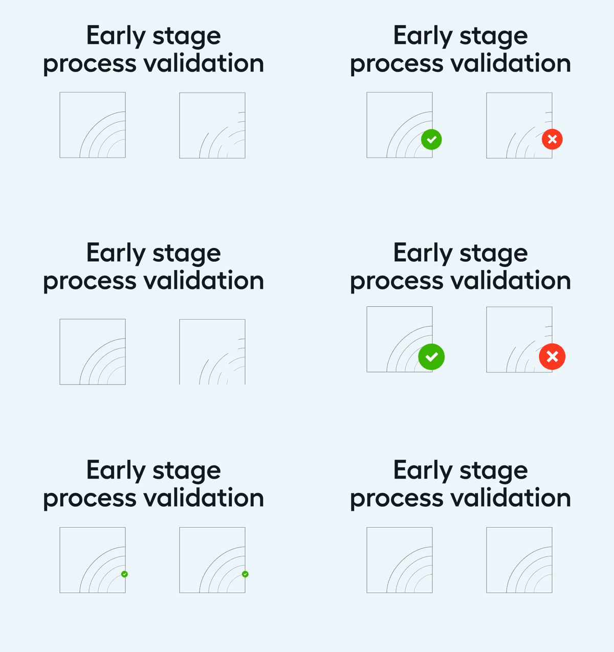
Helios is built to improve the Front End of the Line Photonics wafer processing, by eliminating manual inspection and improving the cleanroom operation time efficiency. Thanks to our high level of automation and intricate AI neural network software. Helios compares die-to-die and identifies missing waveguides in an arrayed waveguide.
Our Photonic visual inspection tool can image the complete wafer. It then processes these defects into an overlay file similar to a GDSII file. Helping the customer to identify the defect sizes and locations.
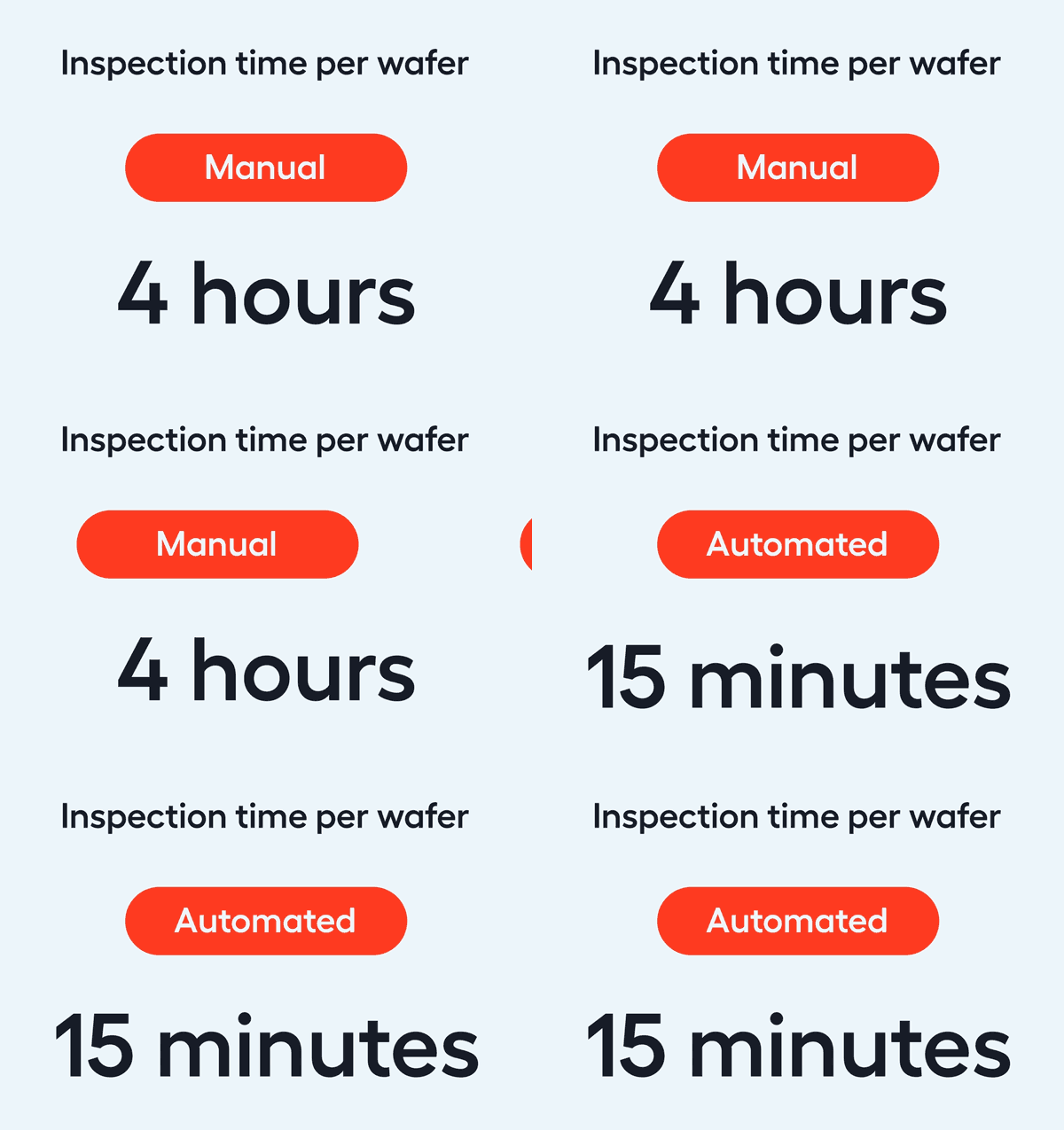
Manual photonic wafer inspection by an operator takes a lot of time. In most cases a single wafer takes approximately 4 hours to inspect. Helios drastically shortens this time by automating this process. It inspects and analyses a wafer in 15 minutes. That is an increase in efficiency of 1600%. Saving valuable time and automating one of the most time consuming tasks.

Compatible with different wafer sizes, Helios is at the top of its league. It has no problems with analysis of 4″, 6″ and 8″ wafers. Wafers are automatically loaded from a SMIF pod, where they are automatically inspected and analyzed based on the operator’s recipe. Viable for various steps in the front end production process. Typically, our Photonic Visual Inspection Tool is used after coating, after litho and after etching.
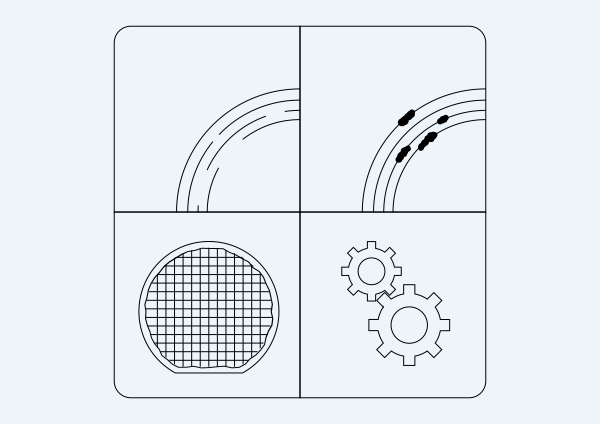
One of the benefits of Helios is automated detection of waveguide interrupts, contaminations, particles and edge cracking. Not all contaminations are defects. With the deep learning annotation tool, Helios can learn what the effects are on PIC functionality and performance. Helios also lets you define own specific issues for automatic detection. Any type of custom contamination can be programmed to make Helios a very flexible machine.
Helios delivers an improved PIC yield because we can detect defects at an early stage. As die defects are successfully identified, an operator can focus on the right areas of the wafer, or cancel the wafer at an early stage. This delivers improved PIC yield and thus drastically lowers costs and time.

The recipe editor of Helios is easy to use. It can be configured to your exact needs and edited for your exact process steps. The recipe editor gives you the opportunity to rapidly work on wafers and scale up wafer inspection.
Retrain algorithms with the annotation tool of Helios. With a deep learning algorithm, annotating becomes much easier. As there are different types of contaminations, the algorithms learn to work with preset standards. These presets are based on your company and your wafers.

 DOWNLOAD
Automated Visual Inspection for Photonic Wafers. Find out everything there is to know about our machine and its possibilities. If you have any questions regarding HELIOS, be sure to get in touch with us.


